Goal
Compute the silicon band structure along the high-symmetry path
L–Γ–X–W–K–Γ and read the indirect gap yourself. Learn tpiba_b path input
and the bands.x post-processor.
scf ─→ calculation='bands' (K_POINTS tpiba_b) ─→ bands.x ─→ plot
New cards and variables
| Item | Role |
|---|---|
calculation='bands' |
Eigenvalues along an arbitrary k-path on a frozen density |
K_POINTS (tpiba_b) |
The path in Cartesian 2π/a units |
bands.x (&BANDS) |
Reorders bands, writes the .gnu file and symmetry labels |
Input files
si.bands.in · si.bandspp.in (the preceding scf is E1's si.scf.in)
The bands run in full:
! E08 step 2: eigenvalues along a high-symmetry path.
! 'bands' is an nscf variant: it reads the scf density of prefix 'si'
! (run E01's si.scf.in first in this directory).

&CONTROL
  calculation = 'bands'
  prefix      = 'si'          ! must match the preceding scf
  outdir      = './tmp/'
  pseudo_dir  = './pseudo/'
  verbosity   = 'high'
/
&SYSTEM
  ibrav       = 2
  celldm(1)   = 10.26
  nat         = 2
  ntyp        = 1
  ecutwfc     = 30
  ecutrho     = 240
  nbnd        = 12            ! bands above the gap, so the conduction bands are plotted
  occupations = 'fixed'
/
&ELECTRONS
  conv_thr    = 1.0d-8
/

ATOMIC_SPECIES
  Si  28.0855  Si.pbe-n-kjpaw_psl.1.0.0.UPF

ATOMIC_POSITIONS (alat)
  Si  0.00  0.00  0.00
  Si  0.25  0.25  0.25

! band path in 'tpiba_b': Cartesian coordinates in units of 2*pi/a.
! each line: k-point, then the number of divisions to the NEXT point
! (the last point gets 0). Path: L - Gamma - X - W - K - Gamma.
K_POINTS (tpiba_b)
6
  0.500 0.500 0.500  30   ! L
  0.000 0.000 0.000  30   ! Gamma
  0.000 1.000 0.000  20   ! X
  0.500 1.000 0.000  20   ! W
  0.750 0.750 0.000  30   ! K
  0.000 0.000 0.000   0   ! Gamma
tpiba_b is Cartesian in 2π/a. QE's primitive-vector convention for
ibrav=2 can differ from the textbook fcc setting, so literature
fractional coordinates pasted into crystal_b produce a wrong path.
When unsure, tpiba_b is the safe choice
(Chapter 10).
The post-processor input:
! E08 step 3: bands.x reorders the raw eigenvalues into continuous bands.
! Products: si.bands.dat (+ .gnu for plotting, .rap with symmetry labels),
! and 'high-symmetry point' lines on stdout that give the x-axis ticks.
&BANDS
  prefix  = 'si'
  outdir  = './tmp/'
  filband = 'si.bands.dat'   ! output basename
  lsym    = .true.           ! classify states by symmetry (writes the .rap file)
/
Run
pw.x    -in si.scf.in     > si.scf.out      # the prerequisite scf (prefix='si')
pw.x    -in si.bands.in   > si.bands.out
bands.x -in si.bandspp.in > si.bandspp.out
The high-symmetry point lines in si.bandspp.out give the tick
positions along the path. Measured: 0.000 (L), 0.866 (Γ), 1.866 (X),
2.366 (W), 2.720 (K), 3.780 (Γ).
Output and figure: measured
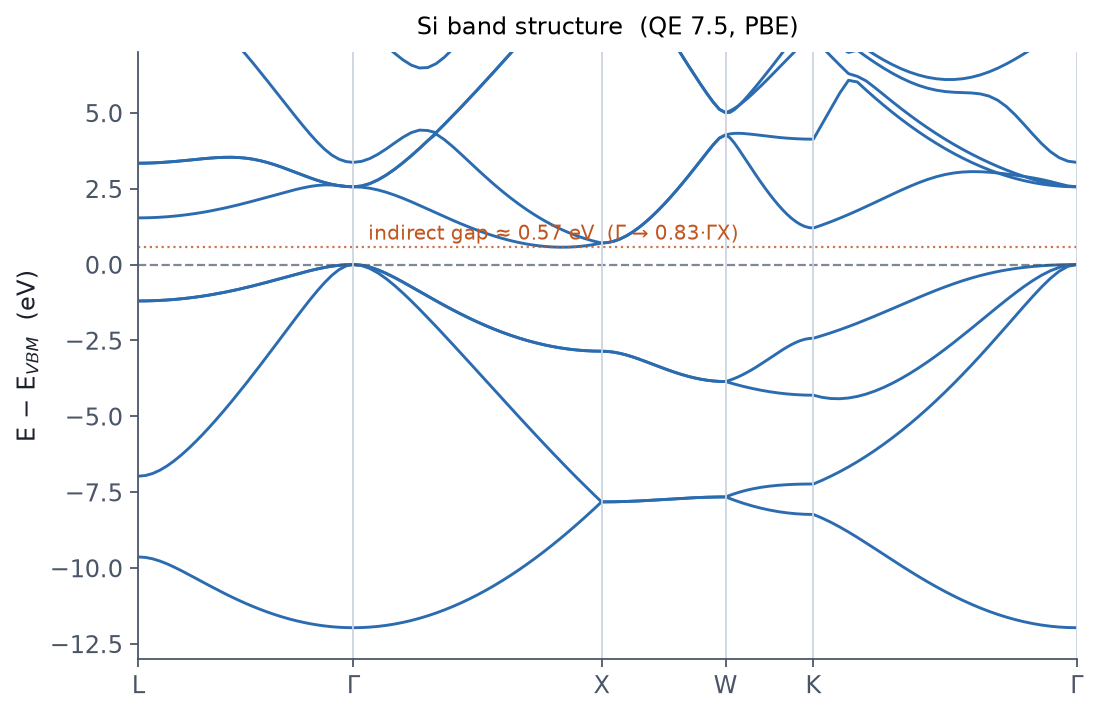
- The zero is the VBM (the scf
highest occupied level, measured 6.212 eV). - Measured indirect gap: 0.57 eV (VBM at Γ, CBM at 0.83 of Γ–X), and a direct gap at Γ of 2.56 eV. The experimental indirect gap is 1.12 eV: the systematic PBE underestimate, on display.
Exercises
- Read both the direct gap at Γ and the indirect gap, and compare.
- Put a nonzero division count on the last path point. What warning do you get?
- Rewrite the same path in
crystal_band check whether the result changes. What is thecrystal_bcoordinate of the L point in QE's fcc convention? - Raise
nbndto 20 and plot the higher conduction bands.
Launching calculation='bands' without the scf: a bands run
builds no density and needs the scf products under the same
prefix/outdir. And a PBE gap below experiment
does not mean your run is broken; it is a
known limitation of the functional. If the gap itself
is the target, move to hybrids or GW.